
Transistor
Transistor nyaéta parangkat sémikonduktor nu miboga tilu terminal, bisa digunakeun keur nguatkeun, nyaklar, nytabilkeun voltase, modulasi sinyal, sarta loba deui kagunaan séjénna. Transistor mangrupa blok wangunan dasar tina integrated circuit (IC) analog atawa digital -- sirkuit nu dipaké ngoperasikeun komputer, telepon sélulér, jeung éléktronika modéren séjénna.
Pangwanoh
[édit | édit sumber]Kecap transistor mangrupa kecap pondokna tina transfer varistor. Dingaranan kitu sabab hiji sinyal asupan digunakeun keur ngarobah résistansi dina jalur sinyal kaluaran (varistor nyaéta variable resistor).
Transistor kabagi jadi dua kategori utama: bipolar junction transistor (BJT) jeung field effect transistor (FET). Panerapan arus dina BJT jeung tegangan dina FET antara asupan jeung terminal common bakal nambah konduktivitas antara terminal common jeung kaluaran, antukna arus pangaturannana ngalir di antarana. Keur leuwih jéntré ngeunaan operasi dua tipe transistor ieu, tempo field effect transistor jeung bipolar junction transistor.
Dina sirkuit analog, transistor dipaké dina panguat, (panguat arus saarah, panguat sora, panguat frékuénsiradio), jeung Sumber daya nu diregulasi linier. Transistor ogé dipaké dina sirkuit digital nu mana fungsina minangka sakelar. Sirkuit digital ngawengku lawang logika, random access memory (RAM), mikroprosesor, jeung pamroses sinyal digital (digital signal processors) (DSP).
|
|
Artikel ieu keur dikeureuyeuh, ditarjamahkeun tina basa Inggris. Bantuanna didagoan pikeun narjamahkeun. |
Pentingna transistor
[édit | édit sumber]The transistor is considered by many to be one of the gréatest inventions in modérn history, ranking in importance with the printing press, automobile and telephone. It is the key active component in practically all modérn electronics. Its importance in today's society rests on its ability to be mass produced using a highly automated process (fabrication) that achieves vanishingly low per-transistor costs.
Although millions of individual (known as discrete) transistors are still used, the vast majority of transistors are fabricated into integrated circuits (also called microchips or simply chips) along with diodes, resistors, capacitors and other electronic components to produce complete electronic circuits. A logic gate comprises about twenty transistors wheréas an advanced microprocessor, as of 2006, can use as many as 1.7 billion transistors (MOSFETs) [1] Archived 2006-10-25 di Wayback Machine.
The transistor's low cost, flexibility and reliability have made it a universal device for non-mechanical tasks, such as digital computing. Transistorized circuits have replaced electromechanical devices for the control of appliances and machinery as well. It is often less expensive and more effective to use a standard microcontroller and write a computer program to carry out a control function than to design an equivalent mechanical control function.
Because of the low cost of transistors and hence digital computers, there is a trend to digitize information. With digital computers offering the ability to quickly find, sort and process digital information, more and more effort has been put into making information digital. As a result, today, much media data is delivered in digital form, finally being converted and presented in analog form by computers. Aréas influenced by the Digital Revolution include television, radio, and newspapers.
Sajarah
[édit | édit sumber]The first patents for the transistor principle were registered in Germany in 1928 by Julius Edgar Lilienfeld. In 1934 German physicist Dr. Oskar Heil patented the field-effect transistor. It is not cléar whether either design was ever built, and this is generally considered unlikely.
On 22 December 1947 William Shockley, John Bardeen and Walter Brattain succeeded in building the first practical point-contact transistor at Bell Labs. This work followed from their war-time efforts to produce extremely pure germanium "crystal" mixer diodes, used in radar units as a frequency mixer element in microwave radar receivers. éarly tube-based technology did not switch fast enough for this role, léading the Bell téam to use solid state diodes instéad. With this knowledge in hand they turned to the design of a triode, but found this was not at all éasy. Bardeen eventually developed a new branch of surface physics to account for the "odd" behaviour they saw, and Bardeen and Brattain eventually succeeded in building a working device.
Bell Telephone Laboratories needed a generic name for the new invention: "Semiconductor Triode", "Solid Triode", "Surface States Triode", "Crystal Triode" and "Iotatron" were all considered, but "transistor," coined by John R. Pierce, won an internal ballot. The rationale for the name is described in the following extract from the company's Technical Memoranda calling for votes:
Transistor. This is an abbreviated combination of the words "transconductance" or "transfer", and "varistor". The device logically belongs in the varistor family, and has the transconductance or transfer impedance of a device having gain, so that this combination is descriptive.
—Bell Telephone Laboratories — Technical Memorandum (May 28, 1948)
Bell put the transistor into production at Western Electric in Allentown, Pennsylvania. They also licensed it to a number of other electronics companies, including Texas Instruments, who produced a limited run of transistor radios as a sales tool. Another company liked the idéa and also decided to take out a license, introducing their own radio under the brand name Sony. éarly transistors were "unstable" and only suitable for low-power, low-frequency applications, but as transistor design developed, these problems were slowly overcome. Over the next two decades, transistors gradually replaced the éarlier vacuum tubes in most applications and later made possible many new devices such as integrated circuits and personal computers.
Shockley, Bardeen and Brattain were honored with the Nobel Prize in Physics "for their researches on semiconductors and their discovery of the transistor effect". Bardeen would go on to win a second Nobel in physics, one of only two péople to receive more than one in the same discipline, for his work on the exploration of superconductivity.
In August 1948 German physicists Herbert F. Mataré (1912– ) and Heinrich Walker (ca. 1912–1981), working at Compagnie des Freins et Signaux Westinghouse in Paris, France applied for a patent on an amplifier based on the minority carrier injection process which they called the "transistron." Since Bell Labs did not maké a public announcement of the transistor until June 1948, the transistron was considered to be independently developed. Mataré had first observed transconductance effects during the manufacture of germanium duodiodes for German radar equipment during WWII. Transistrons were commercially manufactured for the French telephone company and military, and in 1953 a solid-state radio receiver with four transistrons was demonstrated at the Düsseldorf Radio Fair.
-
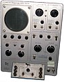 Transistor-curve tracer
 -
 Transistor-curve tracer (detail 1)
 -
 Transistor-curve tracer (detail 2)
 -
 Transistor-curve tracer (parts)


Tipe
[édit | édit sumber] |
PNP |  |
P-channel |
 |
NPN |  |
N-channel |
| BJT | JFET |
Transistors are categorized by:
- Semiconductor material: germanium, silicon, gallium arsenide, silicon carbide
- Structure: BJT, JFET, IGFET (MOSFET), IGBT, "other types"
- Polarity: NPN, PNP, N-channel, P-channel
- Maximum power rating: low, medium, high
- Maximum operating frequency: low, medium, high, radio frequency (RF), microwave (The maximum effective frequency of a transistor is denoted by the term , an abbreviation for "frequency of transition." The frequency of transition is the frequency at which the transistor yields unity gain).
- Application: switch, general purpose, audio, high voltage, super-beta, matched pair
- Physical packaging: through hole metal, through hole plastic, surface mount, ball grid array

Thus, a particular transistor may be described as: silicon, surface mount, BJT, NPN, low power, high frequency switch.
Bipolar junction transistor
[édit | édit sumber]The bipolar junction transistor (BJT) was the first type of transistor to be mass-produced. Bipolar transistors are so named because they conduct by using both majority and minority carriers. The three terminals are named emitter, base and collector. Two p-n junctions exist inside a BJT: the base/collector junction and base/emitter junction. The BJT is commonly described as a current-operated device because the emitter/collector current is controlled by the current flowing between base and emitter terminals. Unlike the FET, the BJT is a low input-impedance device. The BJT has a higher transconductance than the FET. Bipolar transistors can be made to conduct with light (photons) as well as current. Devices designed for this purpose are called phototransistors.
Field-effect transistor
[édit | édit sumber]The field-effect transistor (FET), sometimes called a unipolar transistor, uses either electrons (N-channel FET) or holes (P-channel FET) for conduction. The three main terminals of the FET are named source, gate and drain. On some FETs a fourth connection to the body (substrate) is provided, but normally the body is connected internally to the source.
A voltage applied between the gate and source controls the current flowing between the source and drain. In FETs the source/ drain current flows through a conducting channel néar the gate. This channel connects the source region to the drain region. The channel conductivity is varied by the electric field generated by the voltage applied between the gate/source terminals. In this way the current flowing between the source and drain is controlled. Like bipolar transistors, FETs can be made to conduct with light (photons) as well as voltage. Devices designed for this purpose are called phototransistors.
FETs are divided into two families: junction FET (JFET) and insulated gate FET (IGFET). The IGFET is more commonly known as metal-oxide-semiconductor FET (MOSFET), from their original construction as a layer of metal (the gate), a layer of oxide (the insulation), and a layer of semiconductor. Unlike IGFETs, the JFET gate forms a PN diode with the channel which lies between the source and drain. Functionally, this makes the N-channel JFET the solid state equivalent of the vacuum tube triode which, similarly, forms a diode between its grid and cathode. Also, both devices operate in the depletion mode, they both have a high input impedance, and they both conduct current under the control of an input voltage.
MESFETs are JFETs, in which the reverse biased PN junction is replaced by a semiconductor-metal Schottky-junction. These, and the HEMFETs (high electron mobility FETs), in which a two-dimensional electron gas with very high carrier mobility is used for charge transport, are especially suitable for use at very high frequencies (microwave frequencies; several GHz).
FETs are further divided into depletion-mode and enhancement-mode types. Mode refers to the polarity of the gate voltage with respect to the source at the threshold of conduction. For N-channel depletion-mode FETs the gate is negative with respect to the source while for N-channel enhancement-mode FETs the gate is positive, at the threshold of conduction. For both modes, if the gate voltage is made more positive the source/drain current will incréase. For P-channel devices the polarities are reversed. Néarly all JFETs are depletion-mode types and most IGFETs are enhancement-mode types.
Tipe transistor séjénna
[édit | édit sumber]- Unijunction transistors can be used as simple pulse generators. They comprise a main body of either P-type or N-type semiconductor with ohmic contacts at éach end (terminals Base1 and Base2). A junction with the opposite semiconductor type is formed at a point along the length of the body for the third terminal (Emitter).
- Dual gate FETs have a single channel with two gates in cascode; a configuration that is optimized for high frequency amplifiers, mixers, and oscillators.
- Transistor arrays are used for general purpose applications, function generation and low-level, low-noise amplifiers. They include two or more transistors on a common substrate to ensure close paraméter matching and thermal tracking, characteristics that are especially important for long tailed pair amplifiers.
- Darlington transistors comprise a medium power BJT connected to a power BJT. This provides a high current gain equal to the product of the current gains of the two transistors. Power diodes are often connected between certain terminals depending on specific use.
- Insulated gate bipolar transistors (IGBTs) use a medium power IGFET, similarly connected to a power BJT, to give a high input impedance. Power diodes are often connected between certain terminals depending on specific use. IGBTs are particularly suitable for héavy-duty industrial applications. The Asea Brown Boveri (ABB) 5SNA2400E170100 [2] illustrates just how far power semiconductor technology has advanced. Intended for three-phase power supplies, this device houses three NPN IGBTs in a case méasuring 38 by 140 by 190 mm and weighing 1.5 kg. éach IGBT is rated at 1,700 volts and can handle 2,400 amperes.
- Single-electron transistors (SET) consist of a gate island between two tunnelling junctions. The tunnelling current is controlled by a voltage applied to the gate through a capacitor. [3] Archived 2006-09-24 di Wayback Machine[4]
- Complete list of transistor types T-Transistor.com Archived 2007-03-12 di Wayback Machine
Bahan sémikonduktor
[édit | édit sumber]The first BJTs were made from germanium (Ge) and some high power types still are. Silicon (Si) types currently predominate but certain advanced microwave and high performance versions now employ the compound semiconductor material gallium arsenide (GaAs) and the semiconductor alloy silicon germanium (SiGe). Single element semiconductor material (Ge and Si) is described as elemental.
Characteristics of the most common semiconductor materials used to maké transistors are given in the table below:
| Semiconductor material |
Junction forward voltage V @ 25 °C |
Electron mobility m/s @ 25 °C |
Hole mobility m/s @ 25 °C |
Max. junction temp. °C |
|---|---|---|---|---|
| Ge | 0.27 | 0.39 | 0.19 | 70 to 100 |
| Si | 0.71 | 0.14 | 0.05 | 150 to 200 |
| GaAs | 1.03 | 0.85 | 0.05 | 150 to 200 |
| Al-Si junction | 0.3 | — | — | 150 to 200 |
The junction forward voltage is the voltage applied to the emitter-base junction of a BJT in order to maké the base conduct a specified current. The current incréases exponentialally as the junction forward voltage is incréased. The values given in the table are typical for a current of 1 mA (the same values apply to semiconductor diodes). The lower the junction forward voltage the better, as this méans that less power is required to "drive" the transistor. The junction forward voltage for a given current decréases with temperature. For a typical silicon junction the change is approximately −2.1 mV/°C.
The electron mobility and hole mobility columns show the average speed that electrons and holes diffuse through the semiconductor material with an electric field of 1 volt per méter applied across the material. In general, the higher the electron mobility the faster the transistor. The table indicates that Ge is a better material than Si in this respect. However, Ge has four major shortcomings compared to silicon and gallium arsenide: its maximum temperature is limited, it has relatively high leakage current, it cannot withstand high voltages and it is less suitable for fabricating integrated circuits. Because the electron mobility is higher than the hole mobility for all semiconductor materials, a given bipolar NPN transistor tends to be faster than an equivalent PNP transistor type. GaAs has the fastest electron mobility of the three semiconductors. It is for this réason that GaAs is used in high frequency applications. A relatively recent FET development, the high electron mobility transistor (HEMT), has a heterostructure (junction between different semiconductor materials) of aluminium gallium arsenide (AlGaAs)-gallium arsenide (GaAs) which has double the electron mobility of a GaAs-metal barrier junction. Because of their high speed and low noise, HEMTs are used in satellite receivers working at frequencies around 12 GHz.
Max. junction temperature values represent a cross section taken from various manufacturers' data sheets. This temperature should not be exceeded or the transistor may be damaged.
Al-Si junction refers to the high-speed (aluminum-silicon) semiconductor-metal barrier diode, commonly known as a Schottky diode. This is included in the table because some silicon power IGFETs have a parasitic reverse Schottky diode formed between the source and drain as part of the fabrication process.
Kemasan
[édit | édit sumber]Transistors come in many different packages (chip carriers) (see images). The two main categories are through-hole (or leaded), and surface-mount, also known as surface mount device (SMD). The ball grid array (BGA) is the latest surface mount package (currently only for large transistor arrays). It has solder "balls" on the underside in place of léads. Because they are smaller and have shorter interconnections, SMDs have better high frequency characteristics but lower power rating.
Transistor packages are made of glass, metal, ceramic or plastic. The package often dictates the power rating and frequency characteristics. Power transistors have large packages that can be clamped to heat sinks for enhanced cooling. Additionally, most power transistors have the collector or drain physically connected to the metal can/metal plate. At the other extreme, some surface-mount microwave transistors are as small as grains of sand.
Often a given transistor type is available in different packages. Transistor packages are mainly standardized, but the assignment of a transistor's functions to the terminals is not: different transistor types can assign different functions to the package's terminals. Even for the same transistor type the terminal assignment can vary (normally indicated by a suffix letter to the part number- i.e. BC212L and BC212K).
Panggunaan
[édit | édit sumber]In the éarly days of transistor circuit design, the bipolar junction transistor, or BJT, was the most commonly used transistor. Even after MOSFETs became available, the BJT remained the transistor of choice for digital and analog circuits because of their éase of manufacture and speed. However, the MOSFET has several desirable properties for digital circuits, and since major advancements in digital circuits have pushed MOSFET design to state-of-the-art. MOSFETs are now commonly used for both analog and digital functions.


Saklar
[édit | édit sumber]Transistors are commonly used as electronic switches, for both high power applications including switched-mode power supplies and low power applications such as logic gates.
Panguat
[édit | édit sumber]From mobile phones to televisions, vast numbers of products include amplifiers for sound reproduction, radio transmission, and signal processing. The first discrete transistor audio amplifiers barely supplied a few hundred milliwatts, but power and audio fidelity gradually incréased as better transistors became available and amplifier architecture evolved.
Transistors are commonly used in modérn musical instrument amplifiers, where circuits up to a few hundred watts are common and relatively chéap. Transistors have largely replaced valves in instrument amplifiers. Some musical instrument amplifier manufacturers mix transistors and vacuum tubes in the same circuit, to utilize the inherent benefits of both devices.
Komputer
[édit | édit sumber]The "first generation" of electronic computers used vacuum tubes, which generated large amounts of héat and were bulky, and unreliable. The development of the transistor was key to computer miniaturization and reliability. The "second generation" of computers, through the late 1950s and 1960s féatured boards filled with individual transistors and magnetic memory cores. Subsequently, transistors, other components, and their necessary wiring were integrated into a single, mass-manufactured component: the integrated circuit. Transistors incorporated into integrated circuits have replaced most discrete transistors in modérn digital computers.
Kauntungan transistor dibandingkeun jeung solobong vakum
[édit | édit sumber]Before the development of transistors, vacuum tubes (or in the UK thermionic valves or just valves) were the main active components in electronic equipment. The key advantages that have allowed transistors to replace their vacuum tube predecessors in most applications are:
- Smaller size (despite continuing miniaturization of vacuum tubes)
- Highly automated manufacture
- Lower cost (in volume production)
- Lower possible operating voltages (but vacuum tubes can operate at higher voltages)
- No warm-up period (most vacuum tubes need 10 to 60 seconds to function correctly)
- Lower power dissipation (no héater power, very low saturation voltage)
- Higher reliability and gréater physical ruggedness (although vacuum tubes are electrically more rugged. Also the vacuum tube is much more resistant to nucléar electromagnetic pulses (NEMP) and electrostatic discharge (ESD))
- Much longer life (vacuum tube cathodes are eventually exhausted and the vacuum can become contaminated)
- Complementary devices available (allowing circuits with complementary-symmetry: vacuum tubes with a polarity equivalent to PNP BJTs or P type FETs are not available)
- Ability to control large currents (power transistors are available to control hundreds of amperes, vacuum tubes to control even one ampere are large and costly)
- Much less microphonic (vibration can modulate vacuum tube characteristics, though this may contribute to the sound of guitar amplifiers)
" Nature abhors a vacuum tube " Myron Glass (see John R. Pierce), Bell Telephone Laboratories, circa 1948.
Gallery
[édit | édit sumber]A wide range of transistors has been available since the 1960s and manufacturers continually introduce improved types. A few examples from the main families are noted below. Unless otherwise stated, all types are made from silicon semiconductor. Complementary pairs are shown as NPN/PNP or N/P channel. Links go to manufacturer datasheets, which are in PDF format. (On some datasheets the accuracy of the stated transistor category is a matter of debate.)
- 2N3904/2N3906, BC182 Archived 2008-07-23 di Wayback Machine/BC212 and BC546/BC556: Ubiquitous, BJT, general-purpose, low-power, complementary pairs. They have plastic cases and cost roughly ten cents U.S. in small quantities, making them popular with hobbyists.
- AF107: Germanium, 0.5 watt, 250 MHz PNP BJT.
- BFP183: Low power, 8 GHz microwave NPN BJT.
- LM394: "supermatch pair", with two NPN BJTs on a single substrate.
- 2N2219A/2N2905A: BJT, general purpose, medium power, complementary pair. With metal cases they are rated at about one watt.
- 2N3055/MJ2955: For yéars, the venerable NPN 2N3055 has been the "standard" power transistor. Its complement, the PNP MJ2955 arrived later. These 1 MHz, 15 A, 60 V, 115 W BJTs are used in audio power amplifiers, power supplies, and control.
- 2SC3281/2SA1302: Made by Toshiba, these BJTs have low-distortion characteristics and are used in high-power audio amplifiers. They have been widely counterfeited [5] Archived 2008-12-18 di Wayback Machine.
- BU508: NPN, 1500 V power BJT. Designed for television horizontal deflection, its high voltage capability also makes it suitable for use in ignition systems.
- MJ11012/MJ11015: 30 A, 120 V, 200 W, high power Darlington complementary pair BJTs. Used in audio amplifiers, control, and power switching.
- 2N5457/2N5460: JFET (depletion mode), general purpose, low power, complementary pair.
- BSP296/BSP171: IGFET (enhancement mode), medium power, néar complementary pair. Used for logic level conversion and driving power transistors in amplifiers.
- IRF3710/IRF5210 Archived 2008-12-18 di Wayback Machine: IGFET (enhancement mode), 40 A, 100 V, 200 W, néar complementary pair. For high-power amplifiers and power switches, especially in automobiles.
Pabrik transistor
[édit | édit sumber]- APT Archived 2006-10-16 di Wayback Machine
- Fairchild Semiconductor
- Infineon Technologies
- IRF
- IXYS Corporation
- ON Semiconductor
- Panasonic Semiconductors
- Powerex
- Rohm
- Sanyo Transistors Archived 2006-10-15 di Wayback Machine
- Semikron
- STMicroelectronics
- Toshiba Semiconductor
- Zetex Semiconductors
Tempo ogé
[édit | édit sumber]- Transistor avalans
- Band gap
- Bipolar junction transistor
- Compound transistor
- Transistor Darlington
- Field effect transistor
- FREDFET
- IGBT
- NPN
- PNP
- Sémikonduktor
- Transkonduktansi
- Transrésistansi
- Transistor count
- Modél transistor
- Transistor tilu lawang
- Solobong vakum
- Hukum Moore
- Very-large-scale integration
Référénsi
[édit | édit sumber]Patén
[édit | édit sumber]- U.S. Patent 2524035 — J. Bardeen et. al.
- U.S. Patent 2569347 — W. Shockley
Buku
[édit | édit sumber]- Amos S W & James M R (1999). Principles of Transistor Circuits. Butterworth-Heinemann. ISBN 0-7506-4427-3.
- Horowitz, Paul & Hill, Winfield (1989). The Art of Electronics. Cambridge University Press. ISBN 0-521-37095-7.
- Riordan, Michael & Hoddeson, Lillian (1998). Crystal Fire. W.W Norton & Company Limited. ISBN 0-393-31851-6. The invention of the transistor & the birth of the information age
- Warnes, Lionel (1998). Analogue and Digital Electronics. Macmillan Press Ltd. ISBN 0-333-65820-5.
- Williams, Tim (2001). EMC for Product Designers (3rd edition ed.). Butterworth Heinemann. ISBN 0-7506-4930-5.
Séjénna
[édit | édit sumber]- Armand Van Dormael. "The French Transistor". Proceedings of the 2004 IEEE Conference on the History of Electronics, Bletchley Park, June 2004.
- "Herbert F. Mataré, An Inventor of the Transistor has his moment". The New York Times. Citakan:Citation/showdateError. http://www.mindfully.org/Technology/2003/Transistor-Matare-Inventor24feb03.htm
- Michael Riordan (November 2005). "How Europe Missed the Transistor". IEEE Spectrum 42 (11): 52–57. ISSN 0018-9235.
- C. D. Renmore (1980). Silicon Chips and You.
Tumbu luar
[édit | édit sumber]- AudioUK's Milestones. Photograph of first working transistor
- Transistorized. Historical and technical information from the Public Broadcasting Service
- IEEE Virtual Museum, Let's Get Small: The Shrinking World of Microelectronics. All about the history of transistors and integrated circuits.
- The Transistor Legacy Then and Now Archived 2006-10-13 di Wayback Machine. From Lucent Technologies (Bell Telephone Laboratories/AT&T)
- This Month in Physics History: November 17 to December 23 1947: Invention of the First Transistor Archived 2006-04-22 di Wayback Machine. From the American Physical Society
- 50 Years of the Transistor Archived 2007-07-14 di Wayback Machine. From Science Friday, December 12 1997
- The CK722 Museum. Website devoted to the "classic" hobbyist germanium transistor
- Bob's Virtual Transistor Museum & History Archived 2008-01-21 di Wayback Machine. Treasure trove of transistor history
- 1954 to 2004, the TR-1's Golden Anniversary Archived 2009-06-16 di Wayback Machine. In depth coverage of the Regency radio.
- The Bell Systems Memorial on Transistors.
- Jerry Russell's Transistor Cross Reference Database Archived 2007-02-16 di Wayback Machine.
- Pictures of TO and SOT packages Archived 2006-09-15 di Wayback Machine
- How transistors work
- Transistor Flow Control - Scientific American Magazine (October 2005)